Design of the schematic and board in KiCad.
Using KiCad
I’ve been meaning to learn how to use KiCad for some time and this project seemed to be a perfect excuse. There are few oddities to overcome when using this EDA tool, but I think there are with any. I really like using open source tools, sometimes they require a bit more work and understanding from the user, but they seem to evolve and get a better level of community support than closed source solutions and as this is just a hobby project I appreciate that KiCad is free to use with no restrictions.
Getting started
This blog isn’t going to be a tutorial on how to use KiCad, but the community support for this tool is so good it isn’t hard to find the answers to any questions you have as long as you know what to ask.
I started off this design by searching the part library for the components I was using. The INA226 wasn’t in the standard part library so I thought starting my own library would be a good learning experience. It took me a while to get the search path configuration and setting the “current library” to be used between application working correctly (I found it a bit clunky), but once I did creating a new symbol and footprint was very easy and intuitive.
Schematic capture
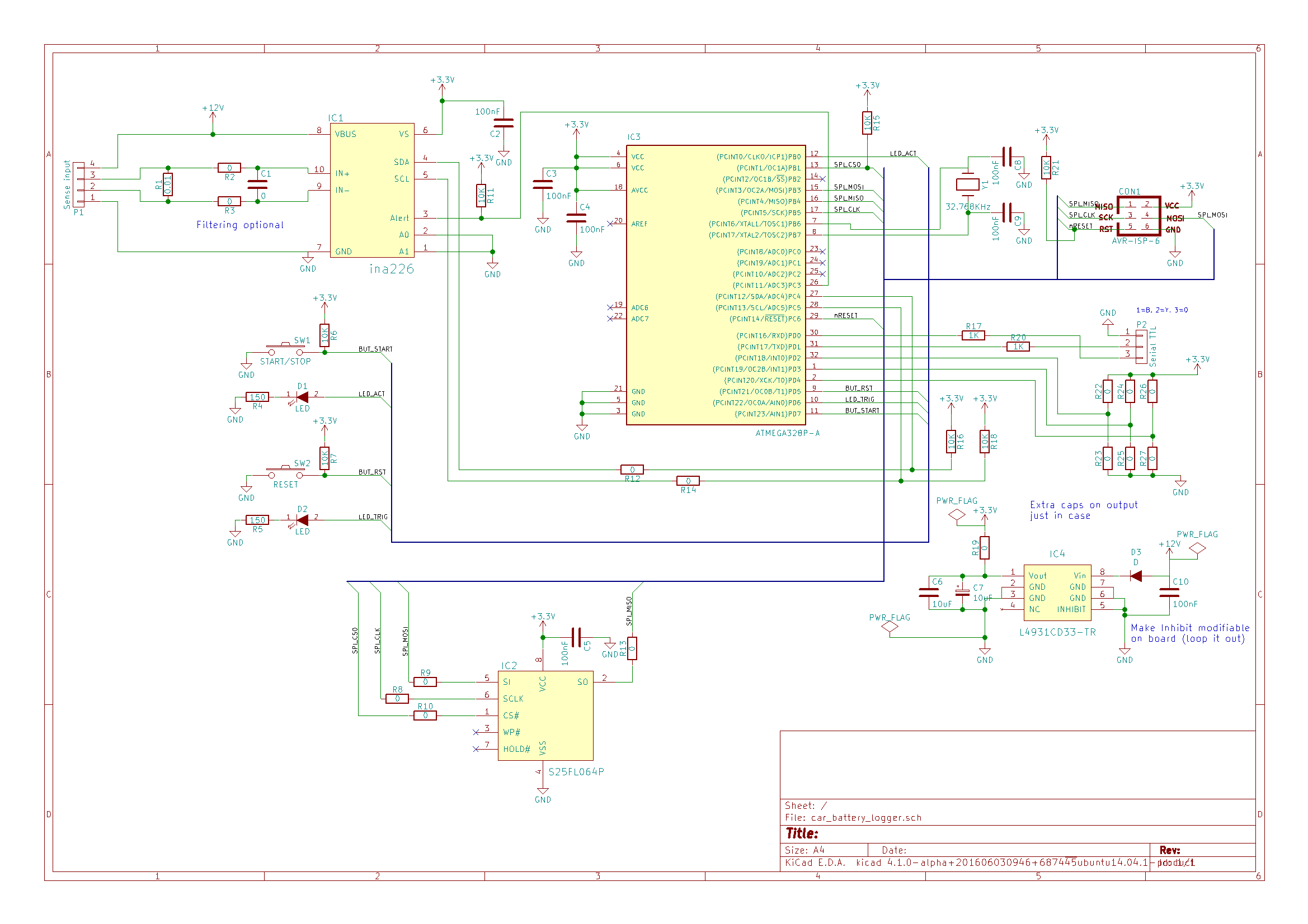
Below is the circuit design for v0.2 of the board. The top left of the schematic is focused on readings from the external shunt resistor, below that are the LED’s and buttons and next to those to the right is the main processor. To the right of the processor is the programming interface, serial interface and some extra IO (currently unused). At the bottom right is the LDO and the bottom left is the flash storage.
There are many optional/unused components in this design which will make the boards much more useful for development. The INA226 has some optional input filtering and an optional local shunt. I have added a number of zero ohm links to the second version of this board to make debugging issues a lot easier, rather than removing IC’s to debug/isolate a problem it’s much easier to remove a resistor. I have also added a few different types of capacitor to the voltage regulator to experiment with different types.
Foot print design
As I intend to build these boards using a soldering iron I chose to make the pads for footprints i’ve created extra long so I could pull any excessive amount of solder away from the other pins, this also helps with getting a better thermal contact between the pad and the soldering iron making soldering with a very fine tip a lot easier.
Board layout
The first thing I did when laying out my board was to find the capabilities of the board manufacturer I was going to use, in my case dirtypcbs and setup my design rules for the board in KiCad. I wanted to keep all of the components on one side and keep the board to two sides to make it cheaper which should be easy given the number of components, it also needed to stay within 5x5cm.
The first board
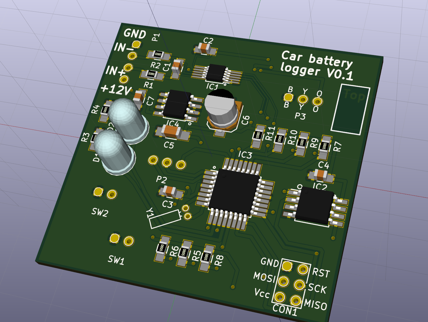
This layout was quite simple, but got a bit messy with the positioning of the components, but I wanted to get this board out to the manufacturer and as they are so cheap I thought the tidy up could wait until the next version, “fail fast” as they say.
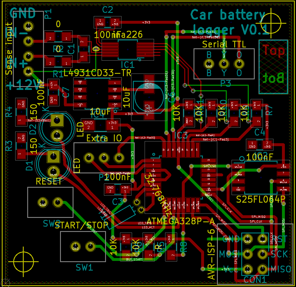 When looking at the rendering you can see the through hole LED’s are massive, I considered using surface mount ones, but I have loads of through hole ones to use up :). I found the ability to render what the assembled board would look like to be very useful, mostly to visualise if the circuit would be buildable with a soldering iron, it’s also easier to see that there is a lot of wasted space on this board.
Then second board
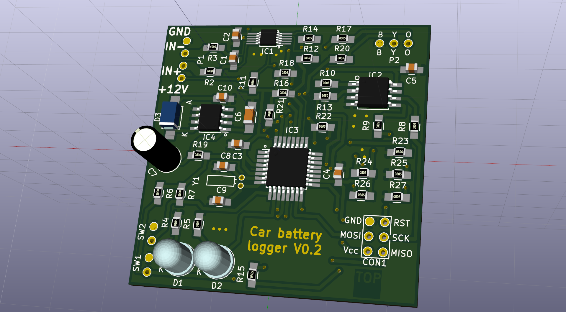
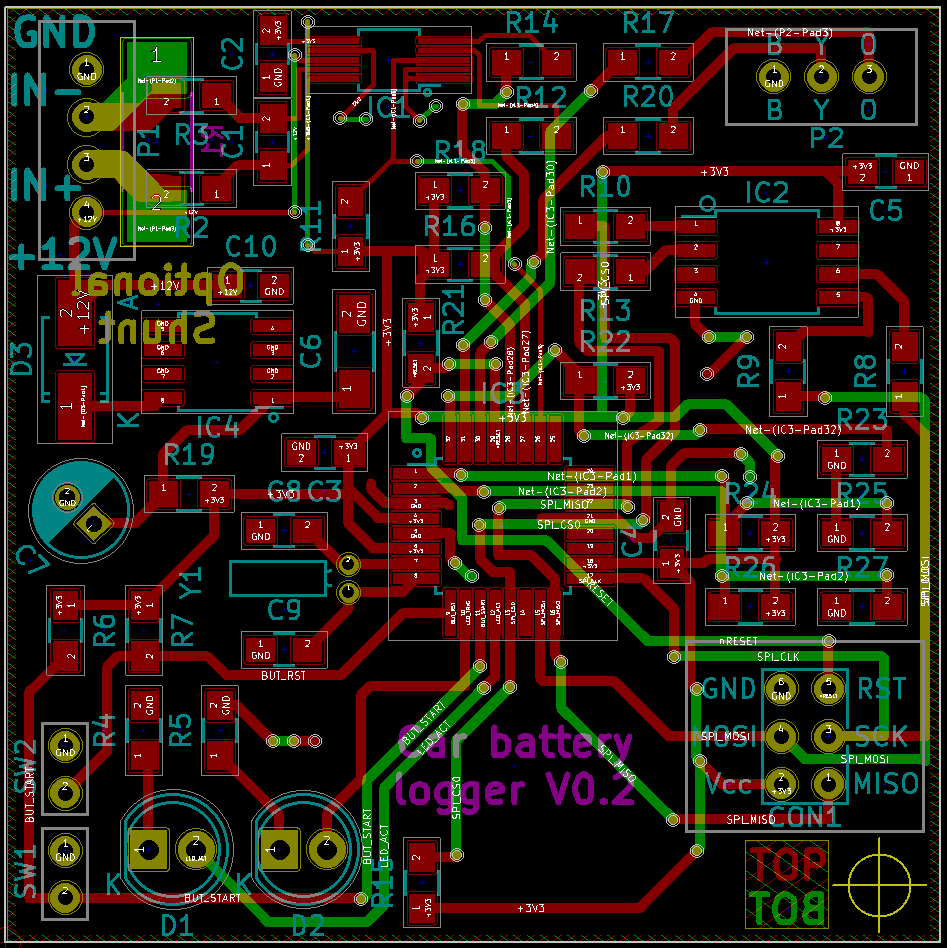
With this version I wanted to address the messiness off the board, this version also had many more optional components to fit in. The biggest problem with the first board was the clearance around pads to the copper pour, as it was such a small clearance and misalignment in the solder mask resulted in potential short when building the circuit, this will be elaborated upon in the next blog post. I’ve also reduced the “courtyard” of a few of my footprints to make things look a bit tidier. There is now an optional onboard shunt resistor, but I had to put it on the back of the board as I was running out of space and it had to be as close as possible to the INA226 for signal integrity reasons. These images showing the board layout don’t show the copper pours (which are all ground pours) which makes the traces like the one above D2 look a bit odd, they are in fact just via stitching, it took me a while to find out that to make those work they have to be connected to ground at one end. The via stitching on this board may have been a bit over the top in places, but the board manufacturer wasn’t going to charge for them and if there were any problems with the plating on any vias this problem should be mitigated with multiple vias. With this version i’ve also put some writing in the solder mask which I thought might look cool, but the end results wasn’t that great so I probably wouldn’t do it again.
 From the rendeding of the second board you can see it’s a lot more densely packed than the first and a lot tidier, the writing in the solder mask wastes quite a lot of space and isn’t really required.